ニュースな英語のホンヤクコンニャク

英語のニュースでお勉強。 知らない単語や表現を、こっそり調べてエラそうに説明してみるブログです。 元の記事から数日遅れることもありますので、ニュースとしては役に立たないこともある。IT系・技術系が主たる対象であります。スパム多過ぎでコメントは承認制にしましたーごめんあそばせー。

Facebookは密かにスマートウォッチを作ってる。来年売り出す計画してる。

Facebook is secretly building a smartwatch and planning to sell it next year

The device would have messaging and fitness features

それはメッセージングとフィットネスの機能を持つようです。

f:id:takamints:20210213130420p:plain
Illustration by James Bareham / The Verge
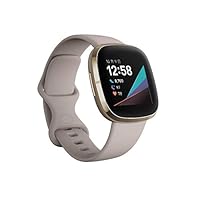


Facebook is building a smartwatch as part of its ongoing hardware efforts, according to a new report from The Information. The device is said to be an Android-based smartwatch, though the report does not say whether Facebook intends for the device to run Google’s Wear OS. It also says Facebook is working on building its own operating system for hardware devices and that future iterations of the wearable may run that software instead.

The Informationから出た新しいレポートによれば、Facebookは自身が進めているハードウェアへの取り組みの一部として、スマートウォッチを作っています。 その機器はアンドロイドベースのスマートウォッチであると言われています。 しかし、このレポートではFacebookがその機器でGoogleの Wear OSを動作させる意図があるとは言っていません。

The smartwatch would have messaging, health, and fitness features, the report says, and would join Facebook’s Oculus virtual reality headsets and Portal video chat devices as part of the social network’s growing hardware ecosystem. Facebook is also working on branded Ray-Ban smart glasses to come out later this year and a separate augmented reality research initiative known as Project Aria, which is part of the company’s broader AR explorations it’s been working on for some time now. Facebook declined to comment regarding any planned smartwatch projects

このスマートウォッチは、メッセージングと健康、そしてフィットネスの機能を持つことになるとレポートは言っています。 そして、ソーシャルネットワークの成長するハードウェアエコシステムの一部として、Facebook の Oculus バーチャルリアリティヘッドセットとPortalビデオチャット機器に組み込まれます。 Facebookは今年後半に出すRay-Banブランドのスマートグラスや、プロジェクトAriaとして知られる、しばらくの間取り組んできた同社の幅広いAR調査の一部である別の拡張現実研究イニシアチブにも取り組んでいます。 Facebookはいかなるスマートウォッチのプロジェクトの計画についてコメントを控えました。

The social networking giant’s hardware ambitions are no secret. The company has more than 6,000 employees working on various augmented and virtual reality projects and as part of existing hardware divisions like Oculus and Portal, as well as experimental initiatives under its Facebook Reality Labs division, Bloomberg reported last month. And although Facebook has not expressed a strong interest in health and fitness devices in the past, the company does have a track record in wearables with its Oculus headsets and forthcoming smart glasses.

ソーシャルネットワーク大手のハードウェアの野心は秘密ではありません。 同社では6千人以上の従業員が、OculusやPortalのような既存のハードウェア事業部の一部として、Facebook Reality Labs 事業部と同様に、様々な拡張および仮想現実プロジェクトに従事していると、Bloombergが先月報告しました。 また、Facebookはこれまで健康とフィットネス機器に強い興味を示しませんでしたが、同社はOculusヘッドセットと今後のスマートグラスを使ったウェアラブルに実績を持っています。

  • a track record - 実績
  • forthcoming - 今後の

Facebook also acquired the neural interface startup CTRL-Labs in 2019. CTRL-Labs specialized in building wireless input mechanisms, including devices that could transmit electrical signals from the brain to computing devices without the need for traditional touchscreen or physical button inputs. The startup’s intellectual property and ongoing research may factor into whatever wearables Facebook builds in the future — including a smartwatch, smart glasses, or future Oculus headsets.

FacebookはまたニューラルインタフェーススタートアップのCTRL-Labs を2019年に買収しています。 CTRL-Labsは無線の入力機構の構築に特化しました。 脳からコンピューティングデバイスへ、従来のタッチスクリーンや物理的なボタンの入力が必要なく、電気信号を送信できる機器を含んでいます。 このスタートアップの知的財産と進行中の研究は、Facebookが将来作るウェアラブル機器がどのようなものであれ、考慮するかもしれません。


元記事は以下からどうぞ。

www.theverge.com

日本の探査機はやぶさ2が小惑星のサンプルを地球へ

Japan's Hayabusa2 probe returns its asteroid sample to Earth

f:id:takamints:20201206191126p:plain
BEHROUZ MEHRI/AFP via Getty Images

Japan’s Hayabusa2 probe has successfully returned an asteroid sample to Earth more than a year after first touching down on Ryugu. JAXA has confirmed that the sample capsule touched down in Australia in the early morning of December 6th local time. The cargo carrier had a relatively lengthy descent, starting its burn through the atmosphere at about 12:28PM Eastern before opening its parachute about 6.2 miles above the Earth and floating gently to terra firma.

日本の探査機「はやぶさ2」が、りゅうぐうに初めて着陸してから1年以上かかって、その小惑星のサンプルを地球へ持ち帰ることに成功しました。 JAXAはサンプルのカプセルが12月6日早朝にオーストラリアに着地したことを確認しました。 このカーゴは、比較的長い降下を行いました。東部時間で午後12時28分頃に、約6.2マイル上空でパラシュートを開く前、大気圏を通って燃え上がり、地上にそっと降り立ちました。

The operation was “perfect,” JAXA said.

「完璧な帰還だった」と、JAXAは言いました。


The probe first landed on Ryugu in February 2019 to capture asteroid material by firing a “bullet” into the surface, kicking up dust and rocks. It was originally supposed to have performed that mission in October 2018, but updated surface data prompted a change in strategy. Hayabusa2 itself will next study the tiny asteroid 1998 KY26, although the probe isn’t expected to arrive until July 2031.

この探査機は、りゅうぐうに2019年の2月にはじめて着陸しました。その表面へ「弾丸」を撃ち込んで、小惑星の素材、舞い上がる塵や砂を採取するためです。 これはもともと2018年10月のミッションで行わたはずでしたが、更新された表面のデータが戦略の変更を示したのです。 はやぶさ2自身は次の調査として、小さな小惑星1998 KY26 へ向かいますので、この探査機は2031年の7月まで戻ってきません。

Provided the asteroid samples pan out as promised, they could be very valuable. Ryugu could help understand the nature of the early Solar System and explore the possibility that asteroids seeded the Earth with organic matter. This won’t be the only mission of its kind, either. NASA’s OSIRIS-REx mission recently captured its own asteroid sample and should return it in September 2023. Don’t be surprised if humanity learns a lot more about its celestial neighborhood in the next few years.

採取した小惑星のサンプルは、とても価値があるものだと約束されています。 りゅうぐうは初期の太陽系を理解するため、そして、小惑星有機物を地球に撒いた可能性を探るために役立ちます。 これは、この種のただ一つのミッションではありません。NASAもまた、OSIRIS-REx ミッションが、その独自の小惑星サンプルを採取し、2023年9月に戻ってきます。 もし人類が今後数年間のうちに隣の天体についてより多くのことを学ぶことになったとして、それは驚くことではありません。


元記事は以下からどうぞ。

www.engadget.com

D-Waveが次世代量子アニーリングチップをリリース

D-Wave releases its next-generation quantum annealing chip

What's it take to make a chip with over a million Josephson junctions?

百万以上のジョセフソン接合でチップを作るために、何が必要なのでしょう?

f:id:takamints:20200930061143p:plain

Today, quantum computing company D-Wave is announcing the availability of its next-generation quantum annealer, a specialized processor that uses quantum effects to solve optimization and minimization problems. The hardware itself isn't much of a surprise—D-Wave was discussing its details months ago—but D-Wave talked with Ars about the challenges of building a chip with over a million individual quantum devices. And the company is coupling the hardware's release to the availability of a new software stack that functions a bit like middleware between the quantum hardware and classical computers.

本日、量子コンピュータ企業 D-Waveが、次世代量子アニーリングの可用性を発表しています。 これは量子効果によって、問題の最適化と最小化を解決することに特化したプロセッサです。 このハードウェア自身は驚きには値しません ― D-Waveは先月この詳細について議論していたため ― しかし、D-Waveは百万以上の量子デバイスによるチップ構築へのこの挑戦について Arsに語りました。 同社は、量子ハードウェアと従来のコンピュータの間でのミドルウェアのように機能する新しいソフトウェアスタックの可用性に、ハードウェアのリリースを結びつけています。


4873119197
動かして学ぶ量子コンピュータプログラミング ―シミュレータとサンプルコードで理解する基本アルゴリズム
Eric R. Johnston(著), Nic Harrigan(著), Mercedes Gimeno-Segovia(著), 丸山 耕司(監修), 北野 章(翻訳)

新品 ¥3,960 5つ星のうち4.0 1個の評価
Amazon.co.jpで詳細を見る


Quantum annealing / 量子アニーリング(量子焼きなまし法)

Quantum computers being built by companies like Google and IBM are general-purpose, gate-based machines. They can solve any problem and should show a vast acceleration for specific classes of problems—or they will, as soon as the gate count gets high enough. Right now, these quantum computers are limited to a few-dozen gates and have no error correction. Bringing them up to the scale needed presents a series of difficult technical challenges.

グーグルやIBMのような企業によって作られてきた量子コンピュータは一般目的のもので、論理回路に基づく機械です。 それらは、あらゆる問題を解くことができます。また、すぐにでも論理ゲートの数が十分に大きくなるため、特定の分野の問題について莫大な加速を見せるはずで、またそうなることでしょう。 現在、これら量子コンピュータは数十の論理ゲートに制限されており、誤り訂正機能がありません。 それらを必要なスケールまで引き上げることは、一連の難しい技術的課題を提示しています。

D-Wave's machine is not general-purpose; it's technically a quantum annealer, not a quantum computer. It performs calculations that find low-energy states for different configurations of the hardware's quantum devices. As such, it will only work if a computing problem can be translated into an energy-minimization problem in one of the chip's possible configurations. That's not as limiting as it might sound, since many forms of optimization can be translated to an energy minimization problem, including things like complicated scheduling issues and protein structures.

D-Waveのマシンは一般目的ではありません。技術的には量子アニーリングを行いますが、量子コンピュータではありません。 このハードウェアの量子デバイスの別の構成に対して、低エネルギー状態を見つける計算を行います。 このように、コンピューティングの問題は、このチップの可能な構成のうちのひとつの中におけるエネルギー最小化問題に変換できる場合にだけ動作します。 これは、想定されるほどの制限ではありません。多くの最適化の形式は、エネルギー最小化問題に変換できるためです。 それには、複雑なスケジューリングやタンパク質の構造などのようなことが含まれます。

※ 以降は原文サイトで確認してください。

>It's easiest to think of these configurations as a landscape with a series of peaks and valleys, with the problem-solving being the equivalent of searching the landscape for the lowest valley. The more quantum devices there are on D-Wave's chip, the more thoroughly it can sample the landscape. So ramping up the qubit count is absolutely critical for a quantum annealer's utility. >This idea matches D-Wave's hardware pretty well, since it's much easier to add qubits to a quantum annealer; the company's current offering has 2,000 of them. There's also a matter of fault tolerance. While errors in a gate-based quantum computer typically result in a useless output, failures on a D-Wave machine usually mean the answer it returns is low-energy, but not the lowest. And for many problems, a reasonably optimized solution can be good enough. >What has been less clear is whether the approach offers clear advantages over algorithms run on classical computers. For gate-based quantum computers, researchers had already worked out the math to show the potential for quantum supremacy. That isn't the case for quantum annealing. Over the last few years, there have been a number of cases where D-Wave's hardware showed a clear advantage over classical computers, only to see a combination of algorithm and hardware improvements on the classical side erase the difference. >### Across generations >D-Wave is hoping that the new system, which it is terming Advantage, is able to demonstrate a clear difference in performance. Prior to today, D-Wave offered a 2,000 qubit quantum optimizer. The Advantage system scales that number up to 5,000. Just as critically, those qubits are connected in additional ways. As mentioned above, problems are structured as a specific configuration of connections among the machine's qubits. If a direct connection between any two isn't available, some of the qubits have to be used to make the connection and are thus unavailable for problem solving. >The 2,000 qubit machine had a total of 6,000 possible connections among its qubits, for an average of three for each of them. The new machine ramps up that total to 35,000, an average of seven connections per qubit. Obviously, this enables far more problems to be configured without using any qubits to establish connections. A white paper shared by D-Wave indicates that it works as expected: larger problems fit in to the hardware, and fewer qubits need to be used as bridges to connect other qubits. >Each qubit on the chip is in the form of a loop of superconducting wire called a Josephson junction. But there are a lot more than 5,000 Josephson junctions on the chip. "The lion's share of those are involved in superconducting control circuitry," D-Wave's processor lead, Mark Johnson, told Ars. "They're basically like digital-analog converters with memory that we can use to program a particular problem." >To get the level of control needed, the new chip has over a million Josephson junctions in total. "Let's put that in perspective," Johnson said. "My iPhone has got a processor on it that's got billions of transistors on it. So in that sense, it's not a lot. But if you're familiar with superconducting integrated circuit technology, this is way on the outside of the curve." Connecting everything also required over 100 meters of superconducting wire—all on a chip that's roughly the size of a thumbnail. >While all of this is made using standard fabrication tools on silicon, that's just a convenient substrate—there are no semiconducting devices on the chip. Johnson wasn't able to go into details on the fabrication process, but he was willing to talk about how these chips are made more generally. >### This isn’t TSMC >One of the big differences between this process and standard chipmaking is volume. Most of D-Wave's chips are housed in its own facility and get accessed by customers over a cloud service; only a handful are purchased and installed elsewhere. That means the company doesn't need to make very many chips. >When asked how many it makes, Johnson laughed and said, "I'm going to end up as the case of this fellow who predicted there would never be more than five computers in this world," before going on to say, "I think we can satisfy our business goals with on the order of a dozen of these or less." >If the company was making standard semiconductor devices, that would mean doing one wafer and calling it a day. But D-Wave considers it progress to have reached the point where it's getting one useful device off every wafer. "We're constantly pushing way past the comfort zone of what you might have at a TSMC or an Intel, where you're looking for how many 9s can I get in my yield," Johnson told Ars. "If we have that high of a yield, we probably haven't pushed hard enough." >A lot of that pushing came in the years leading up to this new processor. Johnson told Ars that the higher levels of connectivity required a new process technology. "[It's] the first time we've made a significant change in the technology node in about 10 years," he told Ars. "Our fab cross-section is much more complicated. It's got more materials, it's got more layers, it's got more types of devices and more steps in it." >Beyond the complexity of fashioning the device itself, the fact that it operates at temperatures in the milli-Kelvin range adds to the design challenges as well. As Johnson noted, every wire that comes in to the chip from the outside world is a potential conduit for heat that has to be minimized—again, a problem that most chipmakers don't face. >### Making software easier >The new chip is being made available at the same time as a major change is coming to the software that controls it. One way to solve problems is to understand the nature of the problem and the hardware at sufficient detail to know how to set the connections on the chip so that the results it returns answer the problem. But that's pretty highly specialized knowledge, and it's outside the sort of expertise most companies have on hand. So D-Wave is attempting to make it easier by providing an intervening software step that gets rid of some of the complexity. >Under the new system, users will have to understand how to convert their problem into something called a "quadratic unconstrained binary optimization," or QUBO. But if they can do that, they can hand the QUBO to something D-Wave is calling its "hybrid problem solver," which will do everything needed to get it to execute on the quantum annealer. >This is part of a general trend toward what have been termed "hybrid solutions" for quantum computing, a trend that's taking place on both the gate-based and annealing platforms. Researchers have acknowledged that the parts of an algorithm that actually perform best on quantum systems are often only a part of a larger computer science problem, and the other parts may perform just fine—or even better—on classical computer hardware. So the full solution to a problem will require a mix of classical and quantum calculations. As is the case here, this can involve using the classical side to figure out how best to program the quantum side. >For D-Wave systems, the possibilities are even more complex. As mentioned above, one of the challenges of exploring energy minimization landscapes on a quantum annealer is figuring out how to fit enough of the landscape into a limited number of qubits. And there are a lot of ways to potentially tackle that issue. Some problems can be divided up into smaller chunks that are then run separately. In other cases, it's possible to examine the QUBO and find ways of optimizing it so that it fits into the available hardware better. >Other solutions involve doing some calculations on each side of the quantum divide. It's possible to do a sparse sampling of the landscape on classical hardware and then get the quantum annealer to focus on those areas that seem to look promising. Alternately, you could use the quantum annealer to sparsely sample and then use the classical computer to exhaustively explore the areas around any low-energy solutions it returns. >New users can worry about all these potential ways of handling their problems if they want to, but they can now simply turn the issue over to the hybrid solver and let it do the worrying for them instead. And D-Wave is hoping that this will vastly expand its potential user base. "There's a lot less work to be done if you don't have to take them all the way down to the machine language and become experts in all the parameter tuning," D-Wave VP of Software Murray Thom told Ars. "Offsetting that to a hybrid solver means that businesses can focus on formulating their problems, getting their preproduction tests done, and solving them at scale." >### But is it faster? >The obvious question left after all of this is whether the new hardware and software is ultimately faster than a purely classical solution. But that's a more complicated question than it initially seems. D-Wave is almost certainly going to be able to identify cases where its hardware outperforms classical algorithms as they now stand. But if the past is any guide, that will motivate computer scientists to give those algorithms a careful look—and possibly find ways of optimizing them further. Performance claims are more of a conversation among experts than they are in the supercomputing space, where there are widely accepted benchmarks. >Perhaps more important is the issue of whether any businesses can find specific cases where the quantum annealing delivers them useful solutions faster than existing algorithms. And that may not require D-Wave's machine to return answers faster in every case than classical algorithms, since businesses may only need to solve problems under a specific set of circumstances. D-Wave's ability to return solutions that may not be the most optimal could provide an advantage, since "really good" may be just as useful for businesses as "the best." >D-Wave is pretty confident that this generation, or possibly the next, will be the point where there's a clear advantage to using its hardware. But evaluating that claim will mean waiting for both users and computer scientists to spend more time on it.

元記事は以下からどうぞ。

arstechnica.com